Fritzing用のパーツをIllustratorで作成する
- created
- 2018-05-25
- last change
- 2018-05-25 02:33:39 +0000
Inkscapeの記事はそれなりにヒットするが・・・
Illustratorに関してはあんまり出てこないので、 作った時に参考にしたサイトをまとめつつ書いてみる。
参考:
- Fritzingパーツ作成方法 | Home Made Garbage
- Fritzing カスタムパーツの作り方 – jumbleat
- Fritzing:パーツ作成1
- Fritzing - Graphic Standards
- Fritzing - Download fonts and templates
- Make Your Own Fritzing Parts - learn.sparkfun.com
作り方は載っているが理由が見当たらない
いろんなサイトに作り方が書かれているけれども、曲りなりにも設計図、 回路図というものが関係してくる。デザインするにも寸法の仕様だとか、 色であるとかが多少は指定されているはずである。
しかし、寸法とか記述の方法とかの根拠がいまいちはっきりしないと思っていたら、 本家のサイトに基本仕様が書かれていた。
基本ルール
Fritzingで回路図を作るためには3つのデータを作らねばならない。
- ブレッドボード用
- 回路図用
- プリント基板用
ブレッドボード用パーツの大きさと色
Grid & Dimensions
In order to fit into the breadboard, Fritzing parts must be designed with a fixed distance of 0.1 inch between the connector pins (legs). Legs dimensions should be 0.03 inch wide and at least 0.03 long.
ブレッドボード用の場合、ブレッドボードに刺さるように ブレッドボード穴のピッチでピンの位置を作図する必要がある。
ブレッドボードの穴の間隔は 0.1inch(2.54mm) である。これは一般的な基板の穴の間隔と同じ。
そしてパーツの足の太さは最大で0.3inch(0.762mm)が推奨サイズである。 また、足の長さも 0.3inch以上 にしておくことが推奨されている。
また、色についても以下のように基準が設定されている
type name color HEX RGB legs grey 8c8c8c 140 140 140 Contacts copper/tinned 9a916c 154 145 108 Cables blue cable 418DD9 65 141 217 blue cable (shadow) 1B5BB3 27 91 179 red cable CC1414 204 20 20 red cable (shadow) 8C0000 140 0 0 black cable 404040 64 64 64 black cable (shadow) 000000 0 0 0 yellow cable FFE24D 255 226 77 yellow cable (shadow) E6AB00 230 171 0 green cable 47CC79 71 204 121 green cable (shadow) 00A63D 0 166 61 grey cable 999999 153 153 153 grey cable (shadow) 666666 102 102 102 white cable FFFFFF 255 255 255 white cable (shadow) 999999 153 153 153 orange cable FF7033 255 112 51 orange cable (shadow) D95821 217 88 33
ほとんどはケーブルの色についてなのであまり必要な情報ではないが、 パーツの足やはんだの色、フットプリントの色などは従っておくべきだろう。

アートボードは作成したパーツと同じサイズにしておくと余分な余白がなくなる
穴のサイズに関しても、だいたい1.1mmぐらいがちょうどよさそう
回路図用のパーツの大きさと色
Fonts
In the Schematics View, Droid Sans is used in different sizes according to the following hierarchy:
Part Name (4,25 points) Pin Label (3,5 points) Pin Group (3,5 points) Pin Number (optional: 2,5 points) Pin Character (3,5 points) - for example PWM
When using a different font, please converted the text into paths, otherwise it won’t be compatible with Fritzing. To restate, if you are using Droid it is not necessary to convert to paths. In general we recommend you use the standard font and keep text as text –we are now beginning to manipulate <text> elements to keep them from mirroring and appearing upside-down when parts are flipped and rotated, and Fritzing looks specifically for <text> elements.
Grid & Dimensions
The fixed distance between the connector pins in the Schematic View is 0.1 inch. Connectors dimensions should be 0,7 points (0,0097 inch) thick and 7,2 points (0,1 inch) long.
We recommend downloading and using our templates as a reference while designing graphics for the Schematic View.
各種ラベルのサイズは
- パーツ名
- 4.25 pt
- ピンラベル
- 3.5 pt
- ピングループ
- 3.5 pt
- ピンナンバー
- 2.5 pt
- ピン特性
- 3.5pt
が基準となる。フォントは Droid Sans を基準にしている。
こちらもピン同士の間隔は 0.1inch(2.54mm) が基準となっている。 ピンの線幅は 0.7pt 、ピンの長さは 0.1inch(2.54mm) を基準とするらしい。
Colors
The part shape and title are in solid black (#000000 or rgb(0, 0, 0)).
Connector pins and their labels are dark grey (#555555 or rgb(85, 85, 85)).
If you group connectors, make the group label a lighter grey (#999999, rgb(153, 153, 153)).
つまりこういうことになる。
| name | color | HEX | RGB |
|---|---|---|---|
| partshape | 000000 | 0 0 0 | |
| title | 000000 | 0 0 0 | |
| connector pin | 555555 | 85 85 85 | |
| pin label | 555555 | 85 85 85 | |
| group label | 999999 | 153 153 153 |

ピンの配置は 左上始まりの 0.1inch(2.54mm) のグリッドに沿うようにするときれいに整う
ピンの外側のアンカー基準で 0.7pt の円を作成しこれを接続口にすると、 画像端から配線が伸びてきれいになる
プリント基板用パーツの大きさと色
Fonts
The PCB footprint should not have any text, as it is dynamically created when working with Fritzing. If you’d still like to add some text, best to use the font “OCR A”.
Dimensions
A Part’s dimensions and distance between connector pins in the PCB View should be exactly as in the real world. This is extremely important for a successful pcb production. We highly recommend checking a part’s dimensions in its datasheet.
Here are a couple of things to keep in mind:
- The stroke of a footprint should be at least 20mils (~0.5mm) thick, otherwise the connection might be ruined while drilling and soldering will be much harder.
- The hole itself should be at least 40mils (~1mm) thick, so you would actually need to create a circle which is at least 60mils (~1.5mm) wide in diameter, because half of the stroke is drawn inside the circle.
- If your part fits on the breadboard, the distance between the footprints should be 100mils (~2.5mm) long.
We also recommend downloading and using our templates as a reference while designing graphics for the PCB View.
実世界のサイズに合うようなパターンを彫らなければならないので、しっかりとサイズを確認すること、 と強く推奨されている。
実際のところ、
- はんだ付けする場所(フットプリント)は 0.5mm 以上ないときびしい
- 穴を開けるパターンの場合、直径1.5mmほど、1.2ptほどの大きさ、線幅にすること
- 丸いパスの大きさで穴を開けるので、線幅の半分は削られてしまうから少し大きめにする
- ブレッドボードに合うサイズの場合、パターン同士の間隔は0.1inch(2.54mm)ほど必要
ということらしい。
Colors
The PCB View uses the following colors:
type name color HEX RGB Connector copper F7BD13 247 189 19 Silkscreen black 000000 0 0 0
こういうことになるらしい。

それぞれ推奨する最小サイズ、ブレッドボードの場合の間隔など
また、プリント基板用のパーツデータにはレイヤー構造にも制約が存在する。

何やらエラーが出る
これはフットプリントのデータが
- copper0
- copper1
- footprint1
- footprint2
- …
- copper1
というグループ/レイヤー構造の中に入っていない場合、エラーとなる。

レイヤー構造をこのようにしなければならない
データのテンプレート
仕様の確認はできた。 では実際にどうやって作ればいいのか、というテンプレートファイルが存在している。
You can download and use these helpful templates to design your custom parts according to Fritzing’s Graphic Standards.
The following .zip file includes:
- Droid Sans font
- OCRA font
- Breadboard View graphics template
- Schematic View graphics template
- PCB View graphics template
最終データ
最終的に作ってみたデータがこちら
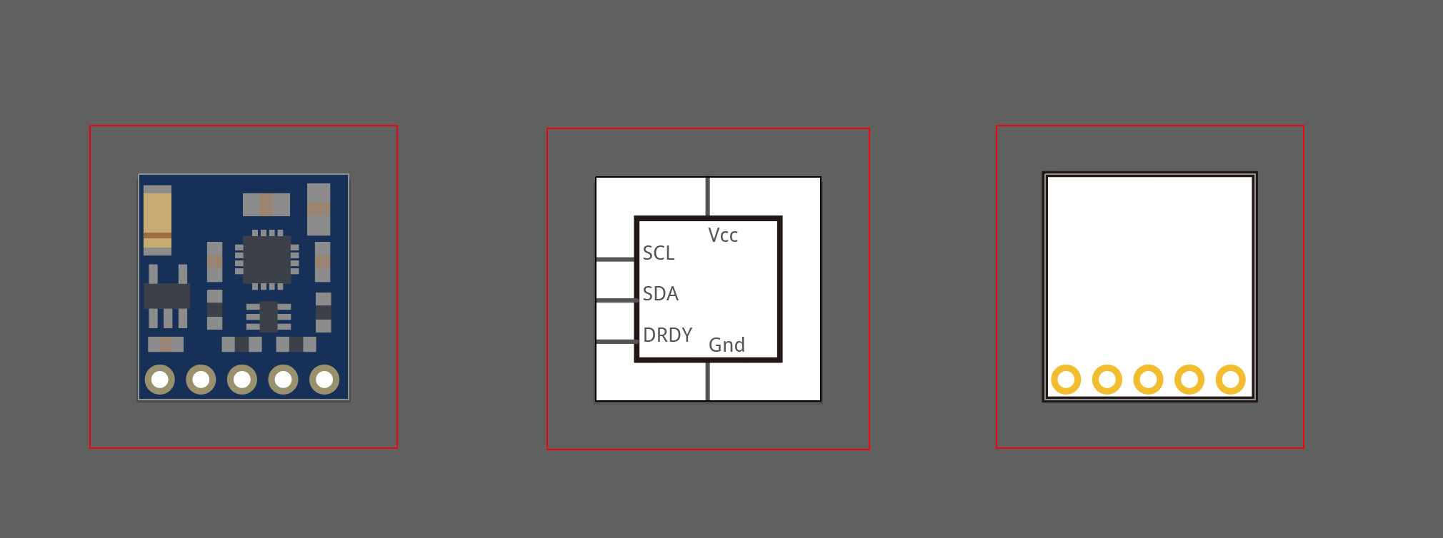
それぞれをSVG出力すれば読み込ませる事ができる
アートボードのサイズは基本的にパーツと同じサイズにしておくこと。
Illustrator CC出力時の設定は以下
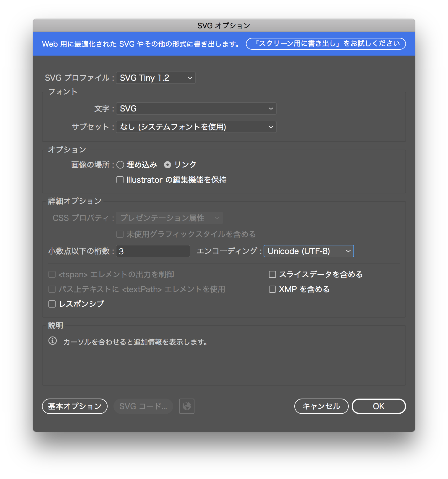
- SVG1.2 Tiny
- レスポンシブのチェックを切る
Thanks to @chidea’s lead, I’ve found a definitive solution. Adobe Illustrator CC has an option (enabled by default) to save SVG as “responsive” (that is, scalable in web pages). Just click on the “More Options” button on the Save pane, while saving as a Tiny 1.2 SVG, and deselect “”esponsive”. Then the file will load correctly with Fritzing without the need to edit it.
Thanks to https://github.com/filamentgroup/grunticon/issues/12713